- 您现在的位置:买卖IC网 > Sheet目录2005 > LTC2262CUJ-14#TRPBF (Linear Technology)IC ADC 14BIT 150MSPS 40-QFN
LTC2262-14
20
226214fc
For more information www.linear.com/LTC2262-14
switching of most of the bits will cause large currents in
the ground plane. By inverting every other bit, the alter-
nate bit polarity mode makes half of the bits transition
high while half of the bits transition low. To first order,
this cancels current flow in the ground plane, reducing
the digital noise.
The digital output is decoded at the receiver by inverting
the odd bits (D1, D3, D5, D7, D9, D11, D13.) The alternate
bit polarity mode is independent of the digital output ran-
domizer—either, both or neither function can be on at the
sametime.Whenalternatebitpolaritymodeison,thedata
format is offset binary and the 2’s complement control bit
has no effect. The alternate bit polarity mode is enabled
by serially programming mode control register A4.
Digital Output Test Patterns
To allow in-circuit testing of the digital interface to the
A/D, there are several test modes that force the A/D data
outputs (OF, D13-D0) to known values:
All 1s: All outputs are 1
All 0s: All outputs are 0
Alternating: Outputs change from all 1s to all 0s on
alternating samples
Checkerboard:Outputschangefrom101010101010101
to 010101010101010 on alternating samples
The digital output test patterns are enabled by serially
programming mode control register A4. When enabled,
the test patterns override all other formatting modes: 2’s
complement, randomizer, alternate-bit-polarity.
Output Disable
The digital outputs may be disabled by serially program-
mingmodecontrolregisterA3.Alldigitaloutputsincluding
OFandCLKOUTaredisabled.Thehighimpedancedisabled
state is intended for long periods of inactivity—it is too
slow to multiplex a data bus between multiple converters
at full speed.
Sleep and Nap Modes
The A/D may be placed in sleep or nap modes to conserve
power. In sleep mode the entire A/D converter is powered
down,resultingin0.5mWpowerconsumption.Sleepmode
is enabled by mode control register A1 (serial program-
ming mode), or by SDI (parallel programming mode).
The amount of time required to recover from sleep mode
depends on the size of the bypass capacitors on VREF,
REFH, and REFL. For the suggested values in Figure 8,
the A/D will stabilize after 2ms.
In nap mode the A/D core is powered down while the
internal reference circuits stay active, allowing faster
wake-up than from sleep mode. Recovering from nap
APPLICATIONS INFORMATION
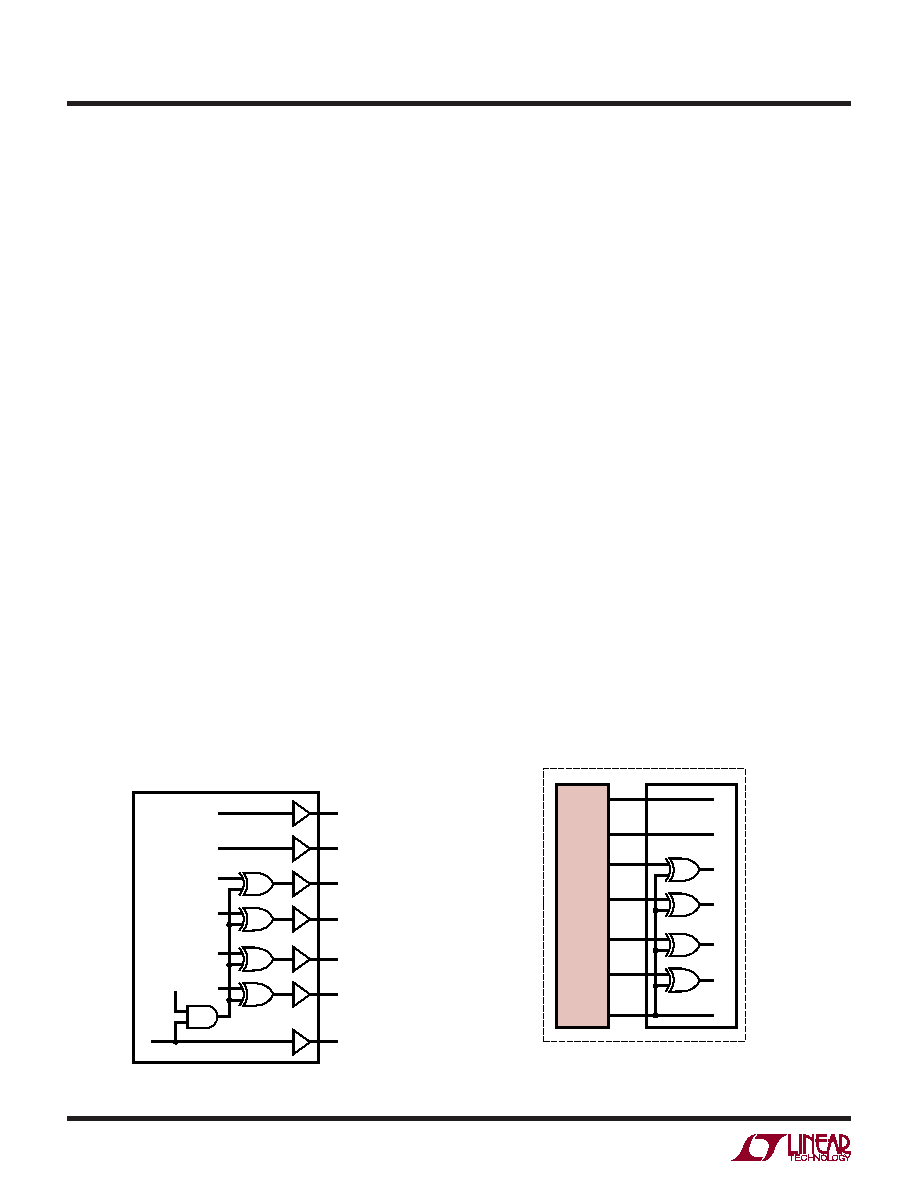
CLKOUT
OF
D13/D0
D12/D0
D2/D0
D1/D0
D0
226214 F15
OF
D13
D12
D2
D1
D0
RANDOMIZER
ON
D13
FPGA
PC BOARD
D12
D2
D1
D0
226214 F16
D0
D1/D0
D2/D0
D12/D0
D13/D0
OF
CLKOUT
LTC2262-14
Figure 15. Functional Equivalent of Digital Output Randomizer
Figure 16. Unrandomizing a Randomized Digital
Output Signal
发布紧急采购,3分钟左右您将得到回复。
相关PDF资料
LTC2262IUJ-12#PBF
IC ADC 12BIT 150MSPS 40-QFN
LTC2264CUJ-12#PBF
IC ADC 12BIT SER/PAR 40M 40-QFN
LTC2268IUJ-14#TRPBF
IC ADC 14BIT 125MSPS DUAL 40QFN
LTC2280CUP#PBF
IC ADC DUAL 10BIT 105MSPS 64-QFN
LTC2281IUP#PBF
IC ADC 10BIT DUAL 64-QFN
LTC2282CUP#PBF
IC ADC DUAL 12BIT 105MSPS 64-QFN
LTC2284CUP#PBF
IC ADC DUAL 14BIT 105MSPS 64-QFN
LTC2285CUP#PBF
IC ADC DUAL 14BIT 125MSPS 64QFN
相关代理商/技术参数
LTC2262IUJ-12#PBF
功能描述:IC ADC 12BIT 150MSPS 40-QFN RoHS:是 类别:集成电路 (IC) >> 数据采集 - 模数转换器 系列:- 标准包装:1 系列:- 位数:14 采样率(每秒):83k 数据接口:串行,并联 转换器数目:1 功率耗散(最大):95mW 电压电源:双 ± 工作温度:0°C ~ 70°C 安装类型:通孔 封装/外壳:28-DIP(0.600",15.24mm) 供应商设备封装:28-PDIP 包装:管件 输入数目和类型:1 个单端,双极
LTC2262IUJ-12#TRPBF
功能描述:IC ADC 12BIT 150MSPS 40-QFN RoHS:是 类别:集成电路 (IC) >> 数据采集 - 模数转换器 系列:- 标准包装:1 系列:- 位数:14 采样率(每秒):83k 数据接口:串行,并联 转换器数目:1 功率耗散(最大):95mW 电压电源:双 ± 工作温度:0°C ~ 70°C 安装类型:通孔 封装/外壳:28-DIP(0.600",15.24mm) 供应商设备封装:28-PDIP 包装:管件 输入数目和类型:1 个单端,双极
LTC2262IUJ-14#PBF
制造商:Linear Technology 功能描述:ADC Single Pipelined 150Msps 14-bit Parallel/LVDS 40-Pin QFN EP 制造商:Linear Technology 功能描述:IC ADC 14BIT 1.8V 150MSPS 40-QFN
LTC2262IUJ-14#TRPBF
制造商:Linear Technology 功能描述:ADC Single Pipelined 150Msps 14-bit Parallel/LVDS 40-Pin QFN EP T/R 制造商:Linear Technology 功能描述:IC ADC 14BIT 150MSPS 40-QFN
LTC2263-12
制造商:LINER 制造商全称:Linear Technology 功能描述:12-Bit, 65Msps/40Msps/25Msps Low Power Dual ADCs
LTC2263-14
制造商:LINER 制造商全称:Linear Technology 功能描述:Quad 14-Bit, 125Msps ADC with Integrated Drivers
LTC2263CUJ-12#PBF
功能描述:IC ADC 12BIT SER/PAR 25M 40-QFN RoHS:是 类别:集成电路 (IC) >> 数据采集 - 模数转换器 系列:- 标准包装:1 系列:microPOWER™ 位数:8 采样率(每秒):1M 数据接口:串行,SPI? 转换器数目:1 功率耗散(最大):- 电压电源:模拟和数字 工作温度:-40°C ~ 125°C 安装类型:表面贴装 封装/外壳:24-VFQFN 裸露焊盘 供应商设备封装:24-VQFN 裸露焊盘(4x4) 包装:Digi-Reel® 输入数目和类型:8 个单端,单极 产品目录页面:892 (CN2011-ZH PDF) 其它名称:296-25851-6
LTC2263CUJ-12#PBF
制造商:Linear Technology 功能描述:IC ADC 12BIT 25MSPS QFN-40